Advanced Packaging Market Size and Share
Market Overview
| Study Period | 2020 - 2031 |
|---|---|
| Market Size (2026) | USD 57.46 Billion |
| Market Size (2031) | USD 90.11 Billion |
| Growth Rate (2026 - 2031) | 9.42% CAGR |
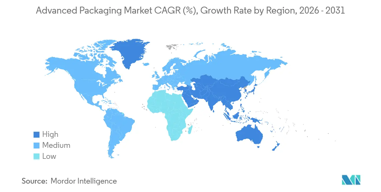
| Fastest Growing Market | Middle East |
| Largest Market | Asia Pacific |
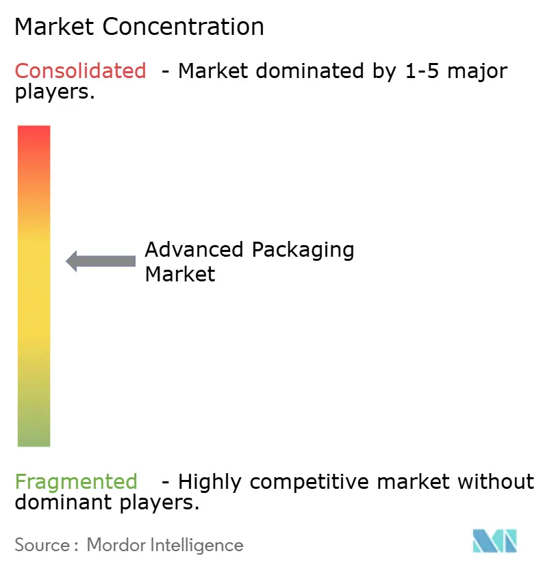
| Market Concentration | Medium |
Major Players *Disclaimer: Major Players sorted in no particular order Image © ���ϲ�����. Reuse requires attribution under CC BY 4.0. | |
Advanced Packaging Market Analysis by ���ϲ�����
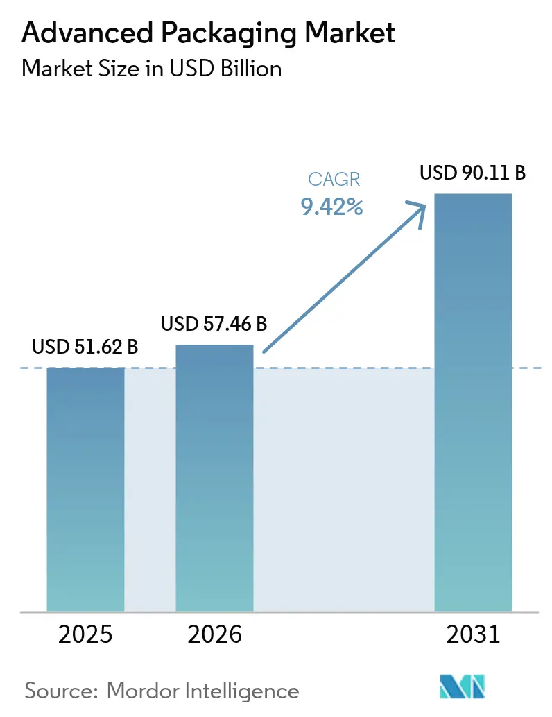
The advanced packaging market size is expected to grow from USD 51.62 billion in 2025 to USD 57.46 billion in 2026 and is forecast to reach USD 90.11 billion by 2031 at 9.42% CAGR over 2026-2031. Momentum is shifting from node-shrink economics to heterogeneous integration, where chiplets, interposers and stacked-die assemblies deliver power-efficient performance that conventional monolithic scaling can no longer support economically. Fan-out wafer-level and 2.5D interposer techniques are gaining importance as sovereign-AI mandates and export-control regimes encourage on-device inference architectures that minimize cross-border technology exposure. Automotive electrification is another structural driver, because silicon-carbide power modules need copper-pillar or hybrid-bond connections to survive thermal cycling far beyond the limits of legacy wire-bond assemblies. Finally, government subsidy programs across the United States, European Union and South Korea are localizing capacity and accelerating equipment purchases that otherwise would have faced multi-year payback hurdles.
Key Report Takeaways
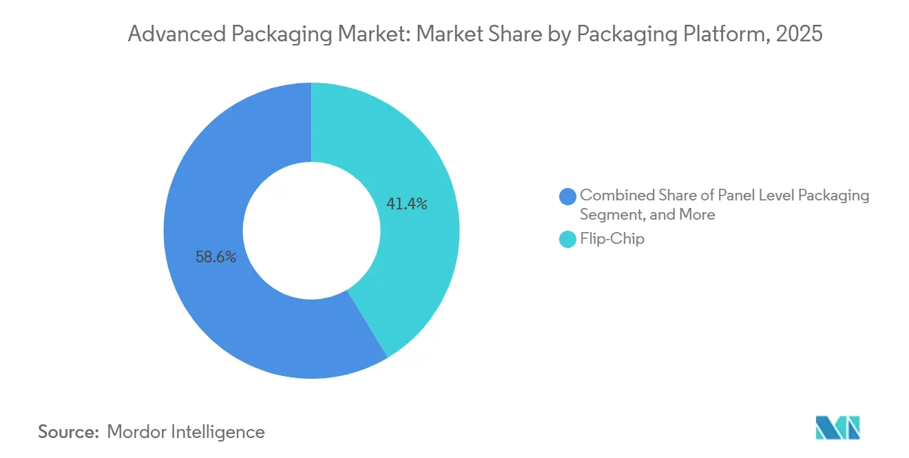
- By packaging platform, flip-chip led with 41.37% of advanced packaging market share in 2025, while panel-level packaging is projected to expand at a 9.72% CAGR through 2031.
- By end-user industry, consumer electronics commanded 48.77% of the advanced packaging market size in 2025; automotive and electric-vehicle applications are advancing at a 10.11% CAGR to 2031.
- By geography, Asia-Pacific accounted for 60.57% of 2025 revenue, whereas the Middle East and Africa region is the fastest, with a 9.61% CAGR forecast to 2031.
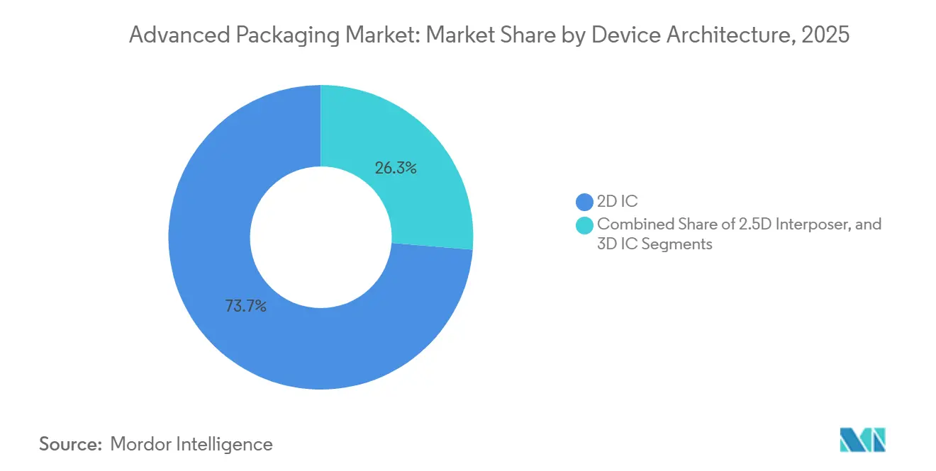
- By device architecture, 2D ICs comprised 73.71% of 2025 shipments; 3D IC designs integrating through-silicon vias are set to grow at 9.55% through 2031.
- By interconnect technology, solder bumps retained 58.92% share in 2025, yet hybrid bonding is on track for a 10.02% CAGR, driven by sub-10-micron pitch demand in AI accelerators.
Note: Market size and forecast figures in this report are generated using ���ϲ�����’s proprietary estimation framework, updated with the latest available data and insights as of 2026.
Global Advanced Packaging Market Trends and Insights
Drivers Impact Analysis*
| Driver | (~) % Impact on CAGR Forecast | Geographic Relevance | Impact Timeline |
|---|---|---|---|
| Rising Demand for Heterogeneous Integration for AI and HPC | +2.1% | Global, with concentration in North America and Asia-Pacific | Medium term (2-4 years) |
| Miniaturization of Consumer Devices Boosting WLP Adoption | +1.6% | Global, led by Asia-Pacific manufacturing hubs | Short term (≤ 2 years) |
| Government Semiconductor Subsidies (CHIPS and EU Chips Acts) | +1.8% | North America and Europe, spillover to allied nations | Long term (≥ 4 years) |
| EV Power-Electronics Reliability Needs | +1.5% | Global, early adoption in Europe and China | Medium term (2-4 years) |
| Emerging Glass-Core Substrates Enabling Panel-Level Packaging | +1.2% | Asia-Pacific core, technology transfer to North America | Long term (≥ 4 years) |
| Co-Packaged Optics Demand in Hyperscale Data Centers | +1.3% | North America and Europe hyperscale clusters | Medium term (2-4 years) |
| Source: ���ϲ����� | |||


Rising Demand for Heterogeneous Integration for AI and HPC
Chiplet architectures now partition logic, memory and I/O across multiple tiles connected by high-bandwidth interposers, enabling compute density that monolithic designs cannot reach within power limits.[1]Taiwan Semiconductor Manufacturing Company, “3D IC and Advanced Packaging,” tsmc.com TSMC shipped more than 15 000 CoWoS wafers in 2025 for NVIDIA’s Hopper and Blackwell GPUs, highlighting commercial readiness. Intel’s Foveros Direct hybrid-bond technology achieves sub-10-micron pitch, cutting cache-to-core latency below 5 ns.[2]Intel Corporation, “Intel Unveils Foveros Direct 3D Packaging Technology,” intel.com Mix-and-match logic, analog and RF tiles fabricated on different nodes optimize cost and time-to-market. The trend sustains double-digit expansion in 2.5D and 3D platforms that underpin data-center accelerators and sovereign-AI initiatives.
Miniaturization of Consumer Devices Boosting WLP Adoption
Smartphones and wearables target sub-6 mm Z-heights, leaving no room for substrate-based packages. Fan-out wafer-level technology redistributes I/O across the die surface, achieving package thickness below 0.4 mm. Apple and Qualcomm have already migrated high-volume processors to fan-out, and mid-tier Android brands follow as tooling costs amortize. Wearable biosensors are adopting fan-in chip-scale packages that eliminate wire bonds, enhancing shock resistance and hermeticity. As brands prioritize thinness and battery life, the advanced packaging market gains incremental wafer-level volume across consumer segments.
Government Semiconductor Subsidies (CHIPS and EU Chips Acts)
The United States CHIPS and Science Act dedicates USD 39 billion in direct grants plus USD 75 billion in loan guarantees, explicitly naming advanced packaging as a strategic capability. TSMC’s Arizona site, backed by USD 6.6 billion in grants, will start CoWoS production in 2025. The EU Chips Act channels EUR 43 billion into regional pilot lines such as Fraunhofer’s panel-level facility in Dresden. South Korea’s KRW 26 trillion package expands Samsung’s Pyeongtaek capacity by 40%. Subsidy competition is redrawing supply chains and fragmenting the advanced packaging market into regional clusters.
EV Power-Electronics Reliability Needs
Silicon-carbide MOSFET inverters face thermal cycles above 200 °C, forcing a move from wire bonds to copper-pillar and hybrid-bond connections that survive 15-year vehicle lifetimes. Infineon’s CoolSiC modules recorded zero field failures across 500 000 vehicles in 2024, validating advanced packaging for automotive power stages.[3]Infineon Technologies, “CoolSiC MOSFET,” infineon.com Tesla’s hybrid-bonded SiC modules cut parasitic inductance 30% and achieved 98.5% inverter efficiency. Automated optical inspection and X-ray laminography raise capex yet shrink warranty reserves, making reliability-centric packaging a core differentiator as battery costs decline.
Restraints Impact Analysis*
| Restraint | (~) % Impact on CAGR Forecast | Geographic Relevance | Impact Timeline |
|---|---|---|---|
| High Capital Intensity of Advanced Packaging Lines | -1.4% | Global, most acute in North America and Europe | Short term (≤ 2 years) |
| Industry Consolidation Squeezing Outsourced Margins | -1.1% | Asia-Pacific OSAT hubs, spillover globally | Medium term (2-4 years) |
| BT-Resin Substrate Capacity Bottlenecks | -0.9% | Global, supply concentrated in Japan and Taiwan | Short term (≤ 2 years) |
| Shortage of Advanced Assembly Talent | -0.8% | North America and Europe, emerging in China | Long term (≥ 4 years) |
| Source: ���ϲ����� | |||
High Capital Intensity of Advanced Packaging Lines
Panel-level factories demand more than USD 500 million per line for lithography, electroplating and test equipment, stretching payback beyond five years at today’s utilizations. Hybrid-bonding tools priced above USD 15 million process only 30 wafers per hour, creating throughput pinch points. Depreciation cycles compress to three years because generations turn quickly, pushing operating margins for many OSATs below 15%. Government subsidies cover only 30–40% of project cost in high-wage regions, forcing private investors to bridge large funding gaps and delaying greenfield expansion.
Industry Consolidation Squeezing Outsourced Margins
Integrated device manufacturers internalize packaging to guard chiplet interconnect IP, reducing third-party volume by double digits in 2025. Samsung bundles I-Cube packaging with foundry wafers, locking customers into single-vendor ecosystems. Amkor and ASE now compete on yield and lead time rather than price alone, yet shrinking customer pools compress negotiating latitude. Smaller OSATs struggle to fund next-generation lines, risking a drop in the number of viable suppliers below 10 by 2028, which could dampen innovation and elevate supply-chain risk.
*Our updated forecasts treat driver/restraint impacts as directional, not additive. The revised impact forecasts reflect baseline growth, mix effects, and variable interactions.
Segment Analysis
By Packaging Platform: Panel-Level Momentum Builds
Panel-level packaging accounted for a modest share in 2025, yet its segment within the advanced packaging market size is projected to expand at a 9.72% CAGR between 2026 and 2031. Flip-chip remained the volume leader with 41.37% of advanced packaging market share in the base year, but its solder-bump pitch cannot drop below 20 µm economically, limiting its future in AI accelerators. Fan-out wafer-level packages thrive in smartphones and wearables, while fan-in WLP supports cost-sensitive RF modules. Embedded-die in PCB laminates attracts automotive radar designers seeking vibration tolerance that offsets a 20% price premium.
The advanced packaging market increasingly views panel-level formats as a route to 40% lower die-handling cost by scaling to 750-mm-square glass substrates whose thermal expansion matches silicon. Equipment maturity remains a gating factor because laser-via drilling, vacuum lamination and large-field step-and-repeat lithography have yet to hit target yields. Commercial readiness is expected after 2027, so supply chains are lining up long-lead tooling orders today. Early adopters focus on data-center processors and AI accelerators where the cost penalty of yield learning curves is amortized over high average selling prices. Until panel platforms scale, flip-chip will keep dominating graphics processors and ASICs albeit with incremental copper-pillar refinements.


By End-User Industry: Automotive and EV Surpass Consumer Electronics
Consumer electronics captured 48.77% of the advanced packaging market size in 2025, yet its unit growth is flattening as smartphone refresh cycles lengthen. Automotive and EV applications are forecast to register a 10.11% CAGR through 2031, the fastest across all industries, reflecting the shift to 800-volt powertrains that rely on silicon-carbide modules packaged with copper pillars and hybrid bonds. Data-center and HPC demand remains robust, fueled by AI inference workloads that exploit chiplet-based GPUs and co-packaged optics.
As battery costs fall and governments impose zero-emission mandates, semiconductor content per vehicle is rising from 5% to 15% of bill-of-materials value, most of which involves advanced packages handling high voltages and harsh thermal cycles. Industrial IoT modules integrate sensors, microcontrollers and radios in system-in-package formats optimized for sub-1 W power envelopes. Healthcare wearables add hermetic fan-in WLP to satisfy biocompatibility. Aerospace and defense, while small, command premium pricing for radiation-hardened, gold-wire packages. The automotive surge ensures that the advanced packaging industry reallocates capex toward power module lines certified under IATF 16949 and ISO 26262.
By Device Architecture: 3D IC Adoption Accelerates
Within the advanced packaging market, 2D ICs still delivered 73.71% of 2025 unit shipments, yet 3D IC designs are projected to grow at 9.55% CAGR to 2031. High-bandwidth-memory stacks bonded atop logic die shrink DRAM latency 70%, enabling real-time inference for large-language models. Intel’s Foveros Direct copper-to-copper hybrid bonding drives 5 ns cache latency and removes solder layers, cutting interface power 15%.
2.5D interposers in GPUs and AI accelerators remain an intermediate architecture because their lateral placement eases thermal management while preserving short paths. Cost-sensitive analog, MCU and RF devices stay on 2D nodes where yields are mature and packaging complexity low. As electronic-design-automation tools mature for multi-die floor-planning and thermal co-simulation, more CPU vendors will disaggregate monolithic dies into chiplets, propelling 3D IC share gains. Ultimately, the balance between yield risk, thermal stacking limits and design-flow availability will dictate the migration tempo across consumer and enterprise segments.
By Interconnect Technology: Hybrid Bonding Challenges Solder Dominance
Solder bumps accounted for 58.92% of 2025 interconnect revenue, but hybrid bonding is forecast to expand at 10.02% through 2031, eroding solder’s lead in the advanced packaging market. Copper-to-copper hybrid bonds enable ≤5 µm pitch and reduce resistance 40%, which translates to double-digit power savings in AI accelerators. Solder bumps continue in cost-driven consumer devices where 40 µm pitch suffices and mechanical compliance is valuable.
Copper pillars, once the main fine-pitch solution for smartphones, bottom out at 20 µm and now serve mid-tier use cases. Oxide-fusion direct bonding demonstrated by Sony achieved 2 µm pitch for stacked CMOS image sensors and hints at future micro-bump-less paths. Each technology now targets distinct performance-cost windows, but as AI inference migrates into broader markets, the industry is converging on hybrid bonding as the default interconnect for logic-to-memory and chiplet networks that demand ultrafine pitch and minimal power loss.
Geography Analysis
Asia-Pacific contributed 60.57% of the advanced packaging market in 2025, reflecting deep clusters of foundries, outsourced assembly and test sites, and substrate makers located in Taiwan, China, South Korea and Malaysia. The region’s dominance is anchored by Taiwan Semiconductor Manufacturing Company’s CoWoS and Samsung’s I-Cube ramps, both of which expanded monthly capacity during 2025 to satisfy AI-accelerator demand. China’s Semiconductor Manufacturing International Corporation and Jiangsu Changjiang Electronics Technology added fan-out wafer-level lines for domestic smartphone and automotive customers, even though export-control limits on extreme-ultraviolet lithography curb their competitiveness at the leading nodes. Japan’s substrate ecosystem, led by Ajinomoto and Ibiden, sustains a resilient material supply chain that underpins the advanced packaging market size for flip-chip and 2.5D modules.
North America is regaining share as the CHIPS and Science Act channels USD 39 billion in grants and USD 75 billion in loan guarantees toward on-shore capacity, explicitly including advanced packaging market infrastructure. TSMC’s Arizona campus begins CoWoS production in 2025, while Intel expands Foveros 3D-packaging lines in New Mexico and Oregon. Amkor’s USD 2 billion Arizona plant focuses on automotive silicon-carbide power modules and aerospace-qualified packages. Canada and Mexico remain limited to back-end test and low-complexity assembly. The advanced packaging market size tied to domestic-content mandates is therefore growing steadily across the continent.
Europe captured modest value in 2025, concentrated in Germany’s Fraunhofer panel-level pilot line and STMicroelectronics assembly in Italy, yet the EU Chips Act’s EUR 43 billion stimulus is set to double regional semiconductor share by 2030. The Middle East and Africa held a small base but is forecast to rise at 9.61% CAGR to 2031 as the United Arab Emirates and Saudi Arabia use sovereign-wealth funds to fund green-field fabs and packaging plants. South America stays limited to test and legacy assembly, with Brazil’s Ceitec serving local automotive suppliers. Overall geographic dispersion reflects customer imperatives to derisk over-reliance on Taiwan, driving the advanced packaging market toward multi-regional redundancy and making site location a competitive differentiator.

Competitive Landscape
Market structure is moderately consolidated, the top five vendors—Taiwan Semiconductor Manufacturing Company, Samsung Electronics, Amkor Technology, ASE Technology and Intel—commanded roughly 55% revenue in 2025, yet more than 20 additional companies remain active, preserving buyer flexibility. Each leading player bundles wafer fabrication with high-density interposer, fan-out or hybrid-bond capacity, capturing a premium for turnkey service that rivals cannot easily match. Samsung integrates I-Cube packaging with foundry wafers, locking customers into a single-vendor path that shields chiplet intellectual property and secures share in the advanced packaging market size.
Outsourced assembly and test providers face margin compression as integrated device manufacturers insource heterogeneous-integration lines. Amkor answers through geographic reach—Arizona for automotive, Portugal for aerospace—and by co-design partnerships that shorten time-to-yield for fabless designers. ASE Technology pairs its Siliconware joint venture with substrate expertise to guarantee supply during BT-resin shortages, a strategy that attracts graphics-processor clients hurt by 2024 material bottlenecks. Powertech Technology and JCET Group occupy specialist niches: automotive-qualified flip-chip for Powertech and fan-out panel-level modules for JCET, both contributing incremental advanced packaging market share while avoiding head-to-head combat with top-tier rivals.
Technology remains the core battlefront. TSMC owns more than 1 200 CoWoS patents, Intel leads copper-to-copper hybrid bonding, and Applied Materials dominates in glass-substrate equipment capable of 2 µm line-and-space resolutions. Start-ups focus on software: Ansys and Cadence extend electronic-design-automation flows that co-optimize multi-die power networks and thermal paths, lowering entry barriers for niche hardware innovators. Competitive intensity therefore hinges on capex scale, patent walls and ecosystem alignment, all of which propel continuous consolidation inside the advanced packaging market.
Advanced Packaging Industry Leaders
Amkor Technology, Inc.
Taiwan Semiconductor Manufacturing Company Limited
Advanced Semiconductor Engineering Inc.
Intel Corporation
JCET Group Co. Ltd
- *Disclaimer: Major Players sorted in no particular order

Recent Industry Developments
- January 2026: TSMC disclosed a USD 2.8 billion CoWoS capacity expansion in Tainan that adds 15 000 wafer starts per month for AI accelerators, with production targeted for Q3 2026.
- December 2025: Samsung Electronics started mass production of I-Cube4, integrating eight high-bandwidth-memory stacks around a logic die with hybrid bonding.
- November 2025: Intel obtained a USD 3.5 billion U.S. Department of Defense contract to deliver Foveros-packaged processors for secure communications.
- October 2025: Amkor finalized a USD 2 billion advanced-packaging plant in Peoria, Arizona, concentrating on silicon-carbide automotive modules.


Global Advanced Packaging Market Report Scope
Advanced packaging refers to the aggregation and interconnection of components before traditional integrated circuit packaging. It allows multiple devices, such as electrical, mechanical, or semiconductor components, to be merged and packaged as a single electronic device. Unlike traditional integrated circuit packaging, advanced packaging employs processes and techniques at semiconductor fabrication facilities.
The Advanced Packaging Market Report is Segmented by Packaging Platform (Flip-Chip, Embedded Die, Fan-in WLP, Fan-out WLP, 2.5D and 3D, System-in-Package, Panel Level Packaging), End-User Industry (Consumer Electronics, Automotive and EV, Data Center and HPC, Industrial and IoT, Healthcare and Med-tech, Aerospace and Defense), Device Architecture (2D IC, 2.5D Interposer, 3D IC), Interconnect Technology (Solder Bump, Copper Pillar, Hybrid Bond, Micro-bump-less Direct Bond), and Geography (North America, South America, Europe, Asia-Pacific, Middle East and Africa). The Market Forecasts are Provided in Terms of Value (USD).
| Flip-Chip |
| Embedded Die |
| Fan-in WLP |
| Fan-out WLP |
| 2.5D / 3D |
| System-in-Package (SiP) |
| Panel Level Packaging (PLP) |
| Consumer Electronics |
| Automotive and EV |
| Data Center and HPC |
| Industrial and IoT |
| Healthcare / Med-tech |
| Aerospace and Defense |
| 2D IC |
| 2.5D Interposer |
| 3D IC (TSV / Hybrid-Bond) |
| Solder Bump |
| Copper Pillar |
| Hybrid Bond |
| Micro-bump-less Direct Bond |
| North America | United States |
| Canada | |
| Mexico | |
| South America | Brazil |
| Argentina | |
| Rest of South America | |
| Europe | Germany |
| United Kingdom | |
| France | |
| Italy | |
| Spain | |
| Rest of Europe | |
| Asia-Pacific | China |
| India | |
| Japan | |
| South Korea | |
| Australia | |
| Rest of Asia-Pacific | |
| Middle East | United Arab Emirates |
| Saudi Arabia | |
| Rest of Middle East | |
| South Africa | |
| Egypt | |
| Rest of Africa |
| By Packaging Platform | Flip-Chip | |
| Embedded Die | ||
| Fan-in WLP | ||
| Fan-out WLP | ||
| 2.5D / 3D | ||
| System-in-Package (SiP) | ||
| Panel Level Packaging (PLP) | ||
| By End-User Industry | Consumer Electronics | |
| Automotive and EV | ||
| Data Center and HPC | ||
| Industrial and IoT | ||
| Healthcare / Med-tech | ||
| Aerospace and Defense | ||
| By Device Architecture | 2D IC | |
| 2.5D Interposer | ||
| 3D IC (TSV / Hybrid-Bond) | ||
| By Interconnect Technology | Solder Bump | |
| Copper Pillar | ||
| Hybrid Bond | ||
| Micro-bump-less Direct Bond | ||
| By Geography | North America | United States |
| Canada | ||
| Mexico | ||
| South America | Brazil | |
| Argentina | ||
| Rest of South America | ||
| Europe | Germany | |
| United Kingdom | ||
| France | ||
| Italy | ||
| Spain | ||
| Rest of Europe | ||
| Asia-Pacific | China | |
| India | ||
| Japan | ||
| South Korea | ||
| Australia | ||
| Rest of Asia-Pacific | ||
| Middle East | United Arab Emirates | |
| Saudi Arabia | ||
| Rest of Middle East | ||
| South Africa | ||
| Egypt | ||
| Rest of Africa | ||


Key Questions Answered in the Report
How large will the advanced packaging market be by 2031?
It is projected to reach USD 90.11 billion by 2031, expanding at 9.42% CAGR from 2026 to 2031.
Which region dominates revenue today?
Asia-Pacific held 60.57% of 2025 revenue thanks to dense manufacturing ecosystems in Taiwan, China and South Korea.
What is the fastest-growing end-user segment?
Automotive and EV applications are forecast to post a 10.11% CAGR through 2031 as silicon-carbide power modules adopt copper-pillar and hybrid bonds.
Why is hybrid bonding important?
It enables ≤5 µm interconnect pitch, lowers resistance 40% and is expanding at 10.02% CAGR, displacing solder bumps in AI accelerators.
How are subsidies reshaping supply chains?
U.S., EU and South Korean incentive programs tie grants to domestic content, driving new CoWoS, Foveros and panel-level lines outside traditional Asia hubs.
What limits small OSAT entrants?
Capital intensity above USD 500 million per panel-level line and rapid depreciation compress margins, making financing difficult without customer prepayments.
Page last updated on:


